
Memory Wipes - Filling in the Gaps
Wiping the NVIDIA BlueField-3 DPU and its BMC. A different architecture to the host tray, wipeable in under 2 hours.
Contents
Memory wipes are one mechanism for ensuring the completeness of inference verification systems. In previous posts we introduced our work on memory wiping:
These posts successfully demonstrated how it is possible to wipe the DDR, GPU HBM, and SSD persistent storage devices of a compute tray. However there are still significant memory stores attached to ancillary devices that are yet to be wiped.
One such device is the Data Processing Unit (DPU) used in the networking implementation of frontier inference compute implementations, such as NVIDIA’s BlueField-3. These devices often use different processor and memory architectures that meaningfully change application of memory wiping.
Device Description
The DPU in our reference machine is an NVIDIA BlueField-3 device (running an Arm Cortex-A78E). The DPU also has its own discrete BMC system (running an Arm Cortex-A7).
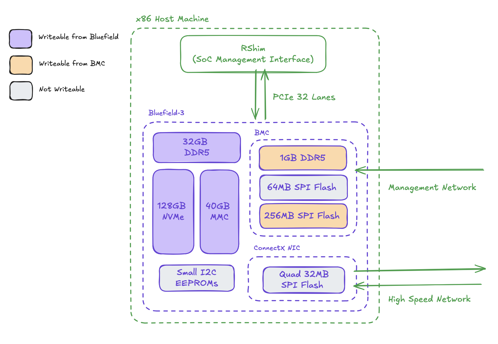
Here is a summary of the memory stores on the DPU along with estimates of how much of that area we believe can be wiped:
| Device | Store | Capacity | Wipeable Memory |
|---|---|---|---|
| DPU | DDR | 32 GB | ≥85% * |
| MMC | 40 GB | ≥99% | |
| NVMe | 128 GB | ≥99% | |
| DPU BMC | DDR | 1 GB | ≥75% * |
| SPI Flash | 64 MB | 0% (Secure Firmware) | |
| SPI Flash | 256 MB | ≥50% ** | |
| ConnectX-7 NIC | SPI Flash | 32 MB | 0% (Secure Firmware) |
| Misc Small EEPROMs | I2C UVPS | 2 Mbit | - |
| I2C FRU | 128 Kbit | - |
Table 1. Estimated wipeability of the DPU's memory stores.
Some of these memory stores cannot be written to due to being protected by one-time-programmable fuses containing secure cryptographic keys, such as the SPI flashes containing the ConnectX firmware and BMC boot ROM. This is a mechanism known as “Secure Firmware” and any data written must be signed by the manufacturer’s private key in order to avoid bricking the device. These memory stores are also resistant to mis-use by the prover for the same reasons.
* System RAM. A portion of this memory will need to be used to hold the OS kernel and the labelling process itself. These figures are a conservative estimate of how much memory we can wipe whilst leaving the kernel with enough operating memory.
** BMC flash. This flash memory device cannot be fully wiped whilst the BMC OS is running, but at least half of it is unused empty space that could be a candidate for wiping.
Other memory stores are outside of our current threat model such as the very small I2C EEPROMs that we think are too small to be useful for attackers.
Experiments
The algorithm for the proof of secure erasure remains the same, but here we are exploring how it can be applied to the DPU and its BMC.
Carving out the DPU’s DDR
To wipe system RAM, we “carve-out” the majority of it, so that the kernel or user processes do not use that section. Unfortunately there is no common mechanism for performing the memory carve-out on all target CPU architectures.
Performing the carve-out is essential for making it safe to label that region without crashing the system.
The DPU’s CPU has a different architecture to the x86-based machine we have previously wiped. There are subtle behavioural differences we have to account for between the architectures:
- On x86 we limit the highest available physical memory address. But labelling of the space above this limit is interfered with when the kernel maps devices in that space. A device mapping is when a memory address leads to an input or output device instead of physical memory.
- On Arm we limit the total aggregate size of the memory regardless of the physical address. This includes all device mappings, so in practice the memory available to the kernel is less than this limit.
In our current implementation, the size of the carved-out area must be carefully tuned to maximise the amount of the labellable memory whilst leaving enough scratch space for the labelling. Scratch is the memory required for intermediate calculations in the labelling process and can be calculated as a function of the amount of intermediate calculations required multiplied by the number of threads performing the labelling.
DPU Persistent Storage
The DPU’s persistent storage appears in Linux as a “block device”, in the same way as in the host. The very high labelling coverage percentage for these devices is achieved by booting the DPU with a custom boot image and running the labelling process completely from within memory.
The DPU’s BMC
The BMC is a more specialised SoC running OpenBMC, a popular embedded Linux distribution for BMCs rather than a general purpose operating system. Wiping the BMC is different from the main DPU system in a few key respects.
Secure Boot and Secure Firmware
There is no way to boot into a custom image like we do with the DPU, as the boot ROM for the BMC is protected by the Secure Firmware mechanism. This means that labelling has to be done from a userspace daemon on the running OpenBMC system.
Another CPU architecture
The BMC is based on the 32-bit Arm Cortex-A7 architecture, so we had to port the wiping system for 32-bit Arm. There are some restrictions that come with this architecture:
-
No Userspace Cache-Flush Instructions: Can’t guarantee labels being written to memory
The instructions we use to flush the CPU cache are privileged on 32-bit Arm CPUs and cannot be executed from the userspace daemon. Flushing the cache is very important! We need to be sure that all labels actually reach the RAM rather than staying in the CPU cache.
In the future, a custom kernel module that allows us to execute privileged instructions could be loaded before labelling begins, to allow the caches to be flushed.
-
No Single Instruction/Multiple Data (SIMD) or Cryptographic Extensions: No hardware acceleration for hashing
There is no hardware acceleration available on this platform for any of our hash algorithms. We can run only the portable C versions of Blake3 or SHA-2. This severely restricts the speed at which we can perform the labelling. However, the small amount of DDR on this device means the labelling speed might not be a problem.
We used Blake3, the faster of the two algorithms on this hardware.
-
Access to Memory Geometry: We must get the extent of the memory in a different way
On SMBIOS-compliant devices such as the x86 host board and the BlueField-3 SoC, we can query the SMBIOS tables for the physical memory geometry. This is the industry standard format for firmware to pass hardware descriptions to the operating system. Using this information we can calculate the labellable areas of DDR by subtracting the System RAM visible to the kernel from the physical memory available on the system.
However, the BMC hardware is defined in advance using Device Tree rather than dynamic discovery exposed by SMBIOS, so the Device Tree must be consulted to find the extent of the physical memory.
Performance Tests
Gamma () is the minimum number of hashes that must be recalculated to recompute a robust label and this must be higher than the number of hashes the prover can perform in the time it takes to get a response to a challenge.
To test performance, we erased a 512 MiB subset of the labellable space with different values of . Larger values here means a deeper, more robust label graph. The impact of on the quality of the proof is discussed in our previous post.
It makes most sense to use the AES algorithm due to the presence of the hardware accelerated cryptographic instructions present on the CPU. These numbers include saturating all 16 cores by using 16 threads to do the labelling.
| Algorithm | Gamma | DDR MB/s | MMC MB/s | NVMe MB/s |
|---|---|---|---|---|
| AES | 4096 | 50.4 | 30.8 | 48 |
| AES | 8192 | 42.8 | 28.8 | 42.8 |
| AES | 16384 | 38.4 | 26.6 | 37.8 |
| AES | 32768 | 33.6 | 24.4 | 33.2 |
| AES | 65536 () | 30.2 | 22.4 | 29.8 |
Table 2. Labelling speeds possible on the DPU.
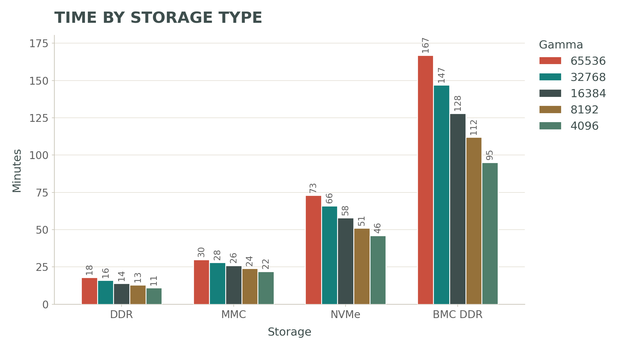
Extrapolating out the performance to the capacity of the memory stores, then the combined time it would take to label the DPU’s memory becomes approximately 2 hours when is at the important threshold of at least . And increasing further to strengthen the proof wouldn’t cost us too much additional time.
On the DPU BMC it makes sense to use the Blake3 algorithm as the fastest algorithm when hardware acceleration is not available. Combined with having only 2 cores, labelling performance was much lower, being measured below 0.1 MB/s. The BMC’s low performance is mitigated by its small memory size, but it still takes a long time as shown in Figure 2.
Conclusions
- A BlueField-3 DPU can be securely wiped in under 2 hours. The DPU is a reasonably performant device and does not have enormous amounts of storage unlike the host tray.
- BMCs are slow. Even though it has very little memory to wipe, it could easily take three hours using the same high value as the DPU.
- The amount of unwiped memory on the BlueField-3 DPU is under 5 GB. Most of which is small capacity EEPROMs, secure firmware flash protected by OTP fuses, or working memory necessary for the labelling process itself.
Future Work
- We are yet to wipe a whole tray all at once. We need to do a comprehensive wipe of all the major tray components such that provers find it impossible to secrete data in one part of the system whilst we wipe another part.
- Investigate performance enhancements and increased labelling coverage. To speed up the labelling of the BMC and increase the amount of memory we can label, we could calculate the labels on the faster host machine.